The advantages and disadvantages of COB encapsulated LED display and its development difficulties
Time:2018-10-09
Views:495
Chip on Board is a kind of structure that installs several LED chips directly on the cooling PCB substrate to conduct heat directly.
COB packaging integrates upstream chip technology, mid-stream packaging technology and downstream display technology. Therefore, drenzer understands that COB packaging requires close cooperation between upstream, middle and downstream enterprises to promote large-scale application of COBLED display.
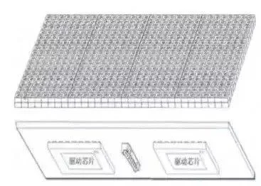
Diagram of COB encapsulated display module
As shown in the figure above, it is a COB integrated encapsulated LED display module, with the LED lamp module as the pixel on the front and the IC drive component at the bottom. Finally, the COB display module is spliced into the designed LED display.
Theoretical advantages of COB:
1. Design and development: without the diameter of a single light body, it can be theoretically made even smaller;
2. Technical process: reduce the cost of supports and simplify the manufacturing process, reduce the thermal resistance of chips, and realize high-density packaging;
3. Engineering installation: from the application side, the COB LED display module can provide easier and faster installation efficiency for the manufacturer of the display application side.
4. Product features:
(1) ultra-thin and thin: according to the actual demand of customers, PCB board with thickness from 0.4-1.2mm can be adopted to reduce the weight to at least 1/3 of the original traditional product, which can significantly reduce the cost of structure, transportation and engineering for customers.
(2) anti-collision and anti-pressure :COB products directly encapsulate the LED chip in the concave lamp position of PCB board, and then use epoxy resin to seal and solidify. The surface of the lamp point is convex into a spherical surface, smooth and hard, and resistant to collision and wear.
(3) big visual Angle: the visual Angle is larger than 175 degrees, close to 180 degrees, and it has better light effect of diffuse color and muddy light.
(4) strong heat dissipation capacity :COB products encapsulate the lamp on the PCB board, rapidly transfer the heat from the wick through copper foil on the PCB board, and the thickness of the copper foil on the PCB board has strict process requirements, coupled with the gold precipitation process, it will hardly cause serious light attenuation.So there are few dead lights, greatly extending the life of the LED display.
(5) wear resistance and easy to clean: the surface is smooth and hard, resistant to collision and wear;Clean with water or cloth without mask.
(6) all-weather excellent features: triple protection treatment is adopted, with outstanding waterproof, moisture, corrosion, dust, electrostatic, oxidation and ultraviolet effect;The temperature difference between minus 30 degrees and 80 degrees can still be used normally.
It is for these reasons that COB encapsulation technology is brought forward in the field of display.
Current technical difficulties of COB:
At present, COB needs to improve its industry accumulation and process details, and also faces some technical difficulties.
1. Low one-time pass rate, low contrast and high maintenance cost;
2. Its color uniformity is far inferior to that of the display screen after SMD device patch with spectroscopic separation.
3. The existing COB packaging still adopts the formal chip, which requires solid crystal and welding line technology. Therefore, there are many problems in the welding line and the process difficulty is inversely proportional to the area of the pad.
4. Manufacturing cost: due to high defect rate, the manufacturing cost is much higher than SMD small spacing.
Based on the above reasons, although the current COB technology has obtained certain breakthrough in the field of display, but doesn‘t mean the SMD technology from declining, in the field of point spacing of 1.0 mm above, SMD packaging technology, with its mature and stable product performance, a wide range of market practice and perfect the security system installation and maintenance of dominant role, user and market direction in the selection of the most suitable.
With the gradual improvement of COB product technology and the further evolution of market demand, the large-scale application of COB packaging technology can reflect its technical advantages and values from the interval of 0.5mm to 1.0mm. To borrow a phrase from the industry, "COB packaging is tailored for the point spacing between 1.0mm and below".Source: drexel
分享


.jpg)


